HackTheBox - Low Logic
---
When we think of CTF, the usual categories revolve around Forensics, Web Exploitation, Cryptography and the likes. However, there is more than that! New categories such as AI, Quantum, Blockchain, etc. have been added by different CTF platforms. One of these is hardware, and today we’ll be tackling an easy level challenge.

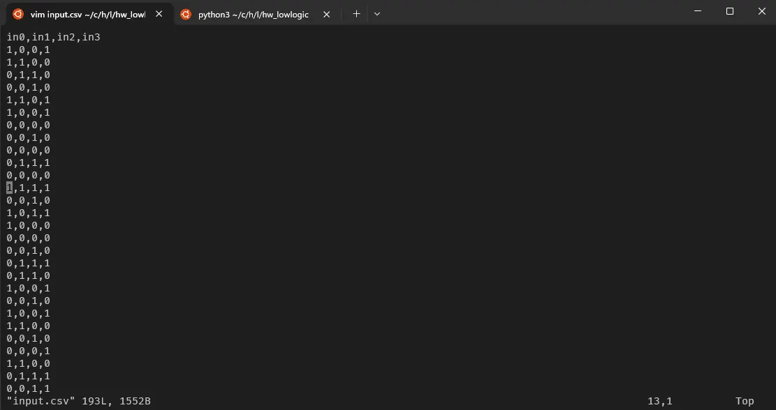
We’re provided with a zip file, containing a schematic diagram and a CSV file filled 24 rows of with binary values with 4 bits each line. They are labeled in0, in1, in2 and in3 respectively.
The schematic diagram looks like this…
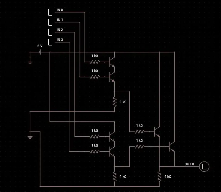
A schematic diagram is simply a 2D diagram with symbols representing different electronic/electrical components describing their layout. It’s essentially like a blueprint for a circuit! In this schematic diagram, we must supply 4 inputs and receive 1 output in return. The bits from input.csv file must be the input for this circuit, and the flag may be extracted from the output.
Here are the 4 basic components found in the schematic diagram
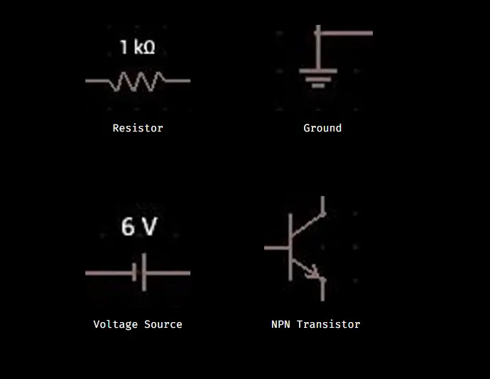
A **resistor** resists the flow of current, in the diagram, it’s used to prevent too much current flowing on the other components.
A **voltage source** or a battery, supplies the circuit with power.
A **ground** is a zero voltage reference, or in this circuit: the negative terminal.
A **NPN transistor** acts like a switch, connecting the Collector leg and Emitter leg when a small current goes through the Base. Transistors are the foundation of computers, you can simulate low-level computer tasks like bit-level arithmetic, latches, and so on and so forth.
If we analyze the schematic diagram, we see that the first two pairs of input are wired through each’s respective transistor’s base. The two transistors are in series with one another, with only the first transistor’s collector connected to the voltage source. The same configuration can also be noticed on the other pair.
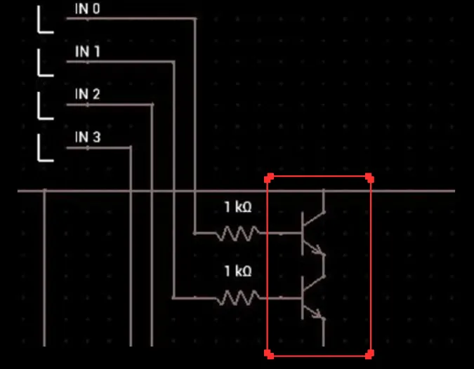
This configuration is an **AND** gate. When both in0 and in1 are turned off, both the transistor are turned off (like a switch), and current cannot pass through, if only the first transistor is turned on, the current travels through it, but gets blocked in the second one. Thus, for the current to continue to the circuit, both must be turned on. Remember that this configuration is also same for the other pair of inputs, so we can visualize this in code:
```
first_pair = in0 and in1
second_pair = in2 and in3
```
Let’s now continue…
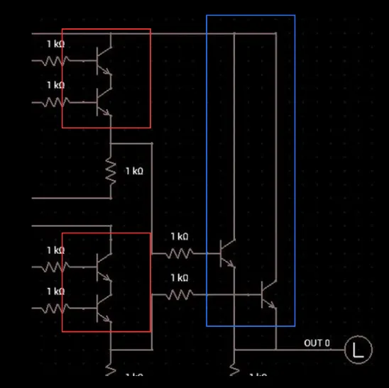
The red box are **AND** gates, the blue one is an **OR** gate. We can tell it is because both transistors are in parallel configuration. This means that even if both or even only one transistor is turned on, current still flows.
If you analyze carefully the output of the 2 **AND** gates are the 2 inputs of the **OR** gate and the output of that **OR** gate is the output. We can visualize this using a logic gate diagram.
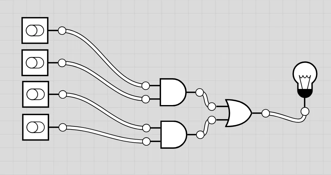
**💡 The output is 1 if at least 1 pair of switches are both turned on.**
Using Python3, we can also simulate this in code…
```
first_pair = in0 and in1
second_pair = in2 and in3
result = first_pair or second_pair
```
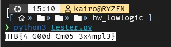
I wrote this code to automatically retrieve the values from the CSV file, convert to binary output into ASCII format and get the flag.

Running this we get…
_But why stop there?!?!?_
I also simulated the circuit in Tinkercad for fun! Check it out [here](https://www.tinkercad.com/things/8v9uQGWBs06-low-logic?sharecode=KYEqXW_IkunL3ZDFU5mvqNLqAPL4iqwOWs1R4yL_83Y)!
**VALUES**: in0 = 1 | in1 = 1 | in2 = 1 | in3 = 0

Thanks for reading!